
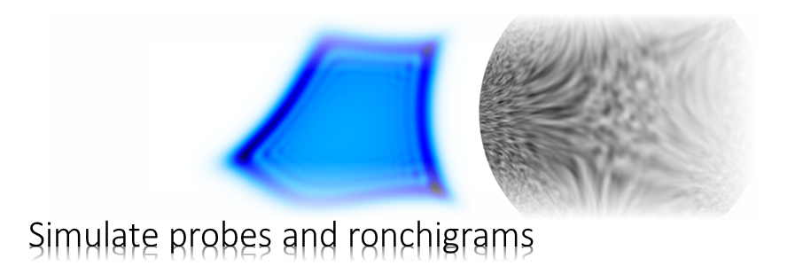
We will simulate the propagation of an electron probe through cubic perovskite SrTiO3 in [001] orientation using the Dr. Probe GUI.
The example builds up on the example for simulating STEM images. Since we will skip detailed explanations and a few steps of the setup in the present example it could be worth to read the previous example.
Quick guide to probe propagation simulations
1. choose the GPU and the number of CPUs to be used (program preferences)
2. set the relevant microscope parameters
2a) accelerating voltage
2b) illumination aperture radius
2c) effective source profile and width
2d) probe aberrations
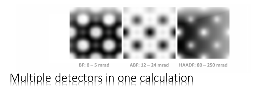
2e) define an auxiliary detector to set the maximum diffraction angle ϑmax
3. prepare object transmission functions (setup sample)
3a) load the structure model
3b) modify the model, reorient & increase size, shift atoms to center of slices
3c) choose number of samples for the simulation grid sufficient to include ϑmax
3d) choose the number of slices matching the number of atomic planes
3e) check the frozen-lattice generation and set the number of variants
4. stack slices periodically to maximum sample thickness
5. prepare the calculation
5a) set sample tilt, thickness step size for readout, and number of repeats per scan position
5b) include partial coherence by simulating focus spread and source size
5c) define a probe position by the scan frame offset
6. choose Probe propagation & CBED as calculation type
7. check that the maximum thickness slider is set to the right value
8. run the multislice calculations
9. view probe intensity (r) and CBED pattern (k) depending on sample thickness
10. save the results
Loading previously saved program parameters and sample structure
In order to make sure that the parameters and appearance of the user interface is similar to this documentation, please download the
Example Setup (file Example02.Setup.zip)
The archive contains a setup file Example02.UISetup.prm for the graphical user interface with all parameters pre-set and a structure model SrTiO3_8x8.cif which we will use for this simulation.
Extract the files from the ZIP archive and load the setup Example02.UISetup.prm using the File / Load Parameters … menu.
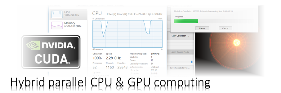
Check the program preferences from the menu Setup / Preferences and select the number of CPUs and the GPU if available on your system. Use not all of the available CPUs. Leave 1 or 2 CPUs to handle the system and calculation manager thread.
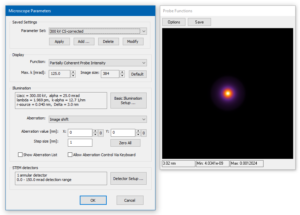
Take a look at the microscope setup. You will find the setup for an aberration corrected 300 kV STEM. The source distribution is set to Lorentz type and an auxiliary detector is defined for the range of diffraction angles up to 150 mrad. This will help us to setup the sampling of the simulation grid.
Preparing object transmission functions
Open the sample setup on the Slice creation page and select the super-cell file SrTiO3_8x8.cif you have downloaded before. You may take a look at the structure, but there is no need to change it for this simulation.
The super-cell contains 8 × 8 × 1 unit cells. Using larger super-cells is beneficial for probe propagation & CBED simulations allowing the probe to spread in a large simulation box without significant periodic wrap-around also for larger sample thickness. Larger cell sizes allow us also to calculate smaller spatial frequencies (smaller diffraction angles), which provides a better resolution of diffraction patterns in the bright-field regime.
Select the Equidistant slicing scheme from the drop-down list and push the button [Suggest Sufficient Sampling]. The program sets the sampling of the super-cell to 729 × 729 pixels and 2 slices. This sampling is sufficient to calculate up to 150 mrad diffraction angles with 300 keV electrons.
Activate the generation of Frozen-lattice configurations and set the number of variants to 100. The slices will occupy about 850 MB computer memory. Start the calculation of phase gratings and wait until it is finished.
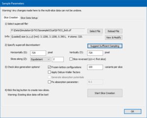
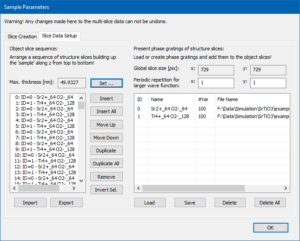
Switch to the page Slice Data Setup and set the maximum sample thickness to 50 nm by clicking on the button [Set]. This will stack the 2 phase gratings in a periodic sequence of 256 sample slices.
Leave the sample setup dialog with the [OK] button and make sure that the maximum thickness slider in the main dialog is set to the rightmost position (49.93 nm thickness, slice #255).
Preparing the calculation
The calculation parameters should already be set up by the previous loading of the GUI setup. You may check it again in the calculation setup by comparing to the images on the right.
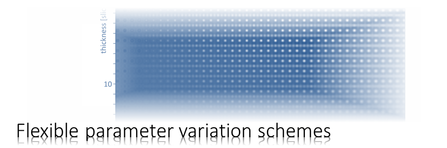
We will simulate probe images for each slice by setting the sample thickness steps to 1.
Using 200 repeats per scan position provides sufficient averaging over random frozen-lattice, focus-spread, and source point variations applied with repeated multislice calculations.
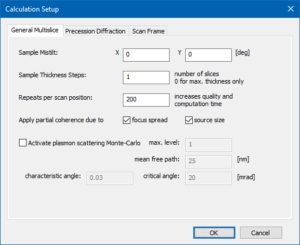
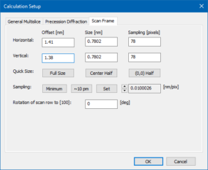
The beam position selected by the scan frame offset corresponds to a point just next to a titanium-oxygen column in the center of the calculation frame. Feel free to change it when repeating the simulation.
Close the calculation setup dialog by pressing the [OK] button.
Running the simulations
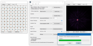
Choose Probe propagation & CBED from the drop-down list of calculation types and push the button [Start Calculation …].
The result type Probe intensity (r) shows the probe intensity distribution at maximum sample thickness. The integration over random frozen-lattice, defocus, and source point variations is updating during the calculation. The total calculation time depends on your hardware. It took less than 3 minutes using 6 CPU threads of an Intel® Core™ i7 with together with a NVIDIA® Quadro® M4000 GPU.
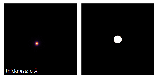
Use the sample thickness slider to see how the probe intensity gets attracted to the Ti-O column and oscillates around it with increasing sample thickness. Significant parts of the probe spread through the crystal filling almost the full simulation box of about 3 nm × 3 nm at 50 nm sample thickness.
Oscillations can also be observed in the CBED patterns, which have been stored as separate result type.
Saving simulation results
There are different ways for saving the current simulation results to files. The most convenient way is using the button [Save Results to File …]. The other way is using the [Save] button of the results display.
The dialog for controlling the saving of results to files is shown in the image above and denotes information regarding the currently selected result in the upper part. It lets you setup file saving options in the lower part.
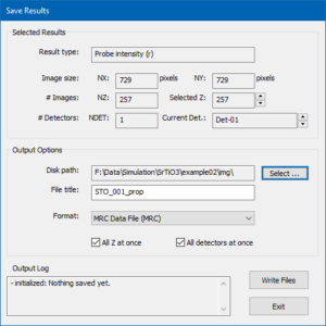

image created with the Gatan Microscopy Suite® 3.21
For the current example, choose an appropriate destination folder (disk path) on your hard drive and enter a file name prefix (file title). Choose the MRC data file format and mark the two check boxes for saving all images of the thickness series at once. Press the [Write Files] button to initiate the saving procedure. A large MRC file should now be saved an can be loaded and displayed again, e.g. using Gatan Microscopy Suite® (GMS2+) by dropping the file into the application window.
You may then inspect the probe intensity distribution from different perspectives, such as the x-z projection shown above. There you can see the oscillation of the electron probe between two sides of the TiO atom column over 50 nm sample thickness.