Follow these examples of image simulations for learning how to use the Dr. Probe software. They may also serve as templates for your own simulations.This document shows how to simulate CBED patterns of body centered cubic iron in [001] orientation of the crystal lattice using the Dr. Probe GUI (version 1.9). This example will show how to get from a very simple structure model of the iron crystal to quite complicated patterns observable in a TEM. CBED patterns are known to be very sensitive to sample thickness and sample tilt and may therefore be used to determine these parameters, e.g. supporting the analysis of high-resolution STEM and TEM images. The simulation will also reproduce the strength and position of Kikuchi lines. However, fine details of the pattern may differ from the experiment because they depend on phonon dispersions which are not taken into account by the simple Einstein model applied in the frozen lattice approximation.
Starting considerations – simulation target
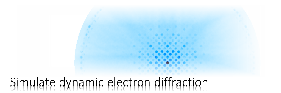
The primary aim of this example is to calculate CBED patterns with sufficient resolution in order to observe details depending on sample thickness and tilt. The maximum scattering angle included will be in the medium range (100 mrad) (i) since intensities become quite low beyond this angle, and a large simulation box is required to obtain a small sampling rate of the diffraction space (k-space). With each calculation we will obtain a series of CBED patterns over thickness, which will include the effects of partial spatial coherence and thermal diffuse scattering (TDS). The example is for a bcc Fe single crystal in [001] zone axis orientation and for a 300 keV electron probe. The CBED patterns will be saved to files on the hard disk in form of raw series data using the MRC file format.
Quick guide to CBED
Here is a short list of points summarizing the way to obtain reasonable CBED patterns:
1. Microscope Setup:
1a) Setup the microscope parameters as usual and as used in the experiment.
1b) In order to be able to use the sampling suggestions of the user interface, setup only one STEM detector covering the detection range from zero to the maximum scattering angle you want to simulate (100 mrad in this example).
2. Sample Setup:
2a) Load the structure model, orient it to the target crystal axis, and increase the x-y size of the model box (a, b) by multiplying. The reciprocal values of the box sizes (1/a, 1/b) determine the resolution of the CBED pattern along each dimension:
Δϑ(a,b) ~ λ Δk(a,b) = λ / (a,b)
2b) Sample and slice the model as suggested by the user interface. Check that each slice corresponds to one atomic plane of the structure. Deviations from the structure plane distances by the slicing will introduce artificial higher-order Laue zones (HOLZ).
2c) Use a sufficient amount (50 – 100) of frozen lattice variants per slice if you want to simulate TDS contributions. For calculating the elastic channel of electron diffraction only, use Debye-Waller factors and absorptive potentials (only one variant required per slice).
2d) Stack the model slices up to the maximum thickness that you want to simulate.
3. Calculation Setup:
3a) Set Sample Thickness Steps to define the series over sample thickness.
3b) Set Repeats per scan position to a large number (≥ 100) to obtain a sufficient average of thermal diffuse scattering and partial coherence effects.
3c) Check to apply partial spatial coherence.
3d) Set the incident probe position by the Scan offset.
4. Select Probe propagation & CBED as calculation type.
5. The CBED pattern (k) output contains the CBED patterns.
PACBED
Position averaged CBED (PACBED) patterns are obtained by increasing the Source Size to large values, e.g. 4 nm. The random variation scheme to simulate partial spatial coherence will then move the probe randomly over a large area leading effectively to position averaging. In order to activate the averaging over the source distribution, the option Apply partial coherence due to: source size must be checked in the Calculation Setup. Due to the random nature of probe positioning in this approach, a large number of position samples (Repeats per scan position) must be used before convergence can be achieved.
Step-by-step setup
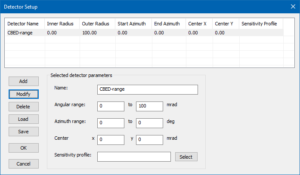
Detector setup for CBED calculations up to 100 mrad.
Microscope parameters
Start the user interface and proceed to the [Microscope Setup]. In the [Basic Illumination Setup] set the accelerating voltage to 300 kV, select a Gaussian source profile and a source size of 0.04 nm (HWHM). We will begin with an illumination aperture of 25 mrad and set the focus spread to 3 nm.
Proceed to the [Detector Setup] and remove all previous detectors. Add a new detector which covers the range from 0 mrad to 100 mrad and give it a name of your choice, e.g. “CBED-range”. The image below shows the detector setup dialog with such a detector definition. Exit the dialog by clicking the [OK] button!
The screenshot on the right shows how the other setup dialogs should look like after finishing the previous steps. Clicking the [OK] button to apply the changed microscope parameters and to return to the Dr. Probe main dialog.
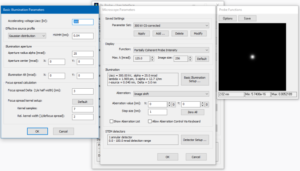
Microscope parameter setup for CBED calculations with a sub-Angstrom, 300-keV electron probe.
Sample setup after loading the initial structure model of bcc Fe.
Sample setup
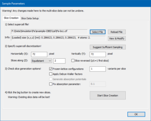
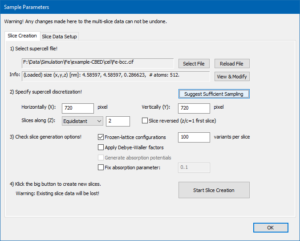
Proceed to the [Sample Setup] and select the Tab <Slice Creation>. Use the [Select File] dialog to load the initial structure model of bcc Fe. The model data is provided here in CIF format;
download: Fe-bcc.cif
and store the file on your computer. The sample setup dialog should now show up similar to the screenshot below.
We will now modify the structure model to the needs for our CBED calculations. Open the [View & Modify] dialog! Keep the initial default crystal orientation of [001] along the beam direction and [010] for the projection y-axis. Change the size of the calculation box by increasing the size of the super cell by a factor of 16 along x and y. This is done by clicking the [Multiply] button in the Projected Cell Size section. An input dialog will ask you to specify three numbers, where you set X = 16, Y = 16, and Z = 1. Apply these factors by clicking the [OK] button, and you return to the [View & Modify] dialog. The new Projected Cell Size should now be 4.58597 nm for the a and b axis of the super cell, while the c axis is still 0.286623 nm. Accordingly, the structure display shows now much more atoms in the x-y projection. The x-z and y-z projections show that there are two atomic planes along the c axis of the super-cell.
Since we will slice the structure model later into two parts along the c axis, one for each of the atomic planes, we will now shift all atoms along z by half an atomic plane, i.e. by a fraction of 0.25 of the current c axis. Click the [Set] button in the section labelled Shift All Atoms [u’v’w’], and define the shift vector in fractional coordinates of the current (!) super-cell with X = 0, Y = 0, and Z = 0.25!
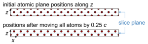
x–z projections of the extended bcc Fe structure model with the recommended shifting of the atomic planes. The atomic planes along the slicing axis (z) should be placed well between the slicing planes in order to prevent numerical round-off errors.
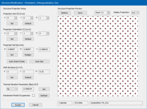
Dialog for sample structure modifications with the above steps applied.
With this shift, the atomic sites will be placed well in between the slice planes as shown in lower part of the above image. This prevents possible numerical round-off errors in the slicing procedure, where each atom is assigned to one structure slice. It is in general recommended to take care of this problem: Ideally, the atomic planes should have a noticeable distance from the slice planes. Atomic sites assigned to the wrong slice may lead to significant errors in dynamic electron diffraction.
The Structure Modification dialog should now show up like in the screenshot on the left. You may want to [Save] the modified structure in a new CIF file to load it again later. Click the [Accept] button to apply the changes and return to the Sample Setup dialog.
We will now set the parameters for the structure slicing and of the numerical calculation grid. First, select the “Equidistant” slicing scheme if not done so already, then press the button [Suggest Sufficient Sampling]! This should automatically fill optimum numbers for the horizontal (X), vertical (Y), and slicing (Z) discretization of the super-cell. In the present case 720 samples along X and Y, and 2 slice planes will be used. Changing the accelerating voltage, maximum detection range limit, and super-cell size will lead to different optimum numbers. In order to include thermal diffuse scattering (TDS), check the Frozen-lattice configurations and set the number of variants per slice to 100 in the slice generation options! When your <Slice Creation> dialog looks like the screenshot above, you should press the big [Start Slice Creation] dialog. The popup dialog will inform you on the progress of the calculation. This will take about one minute or more, depending on available CPU power and the number of used CPU threads (see program preferences).
Setup of the slice data stacking realizing a periodic crystal of 50 nm maximum thickness for the multislice calculation.
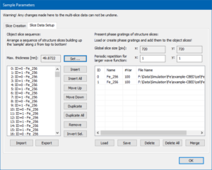
After the slice calculation is finished, you should proceed to the Tab <Slice Data Setup> of the Sample Parameters dialog. The two lists should show two items right now, one for each slice plane. The list on the right side represents the slice data that you just created, while the left list represents the object slice stack, where you can insert present slice data realizing a crystal of some thickness. In order to set up a periodic crystal from the available slice data, click the [Set] button next to the Max. Thickness display. A dialog will open and ask you to set the maximum sample thickness for the simulation. Enter 50 nm and apply this value by pressing the [OK] button. The left list should now be filled with 348 slices in the sequence 0, 1, 0, 1, … referring to the slice data of the right list. The maximum sample thickness of the calculation is now displayed as 49.8722 nm, as shown in the screenshot on the left.
With this step the sample setup is finished and you should now return to the main dialog by pressing the [OK] button.
Calculation setup
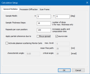
Open the Calculation Setup dialog to define a few parameters relevant for the multislice calculation of CBED patterns. Select the General Multislice tab and set the Sample Mistilt to the default values of (0, 0) deg. We will generate an image series over sample thickness by defining periodic readout steps (Sample Thickness Steps) with 16 slices (2.3 nm). Also set the number of Repeats per scan position to 100 for averaging over frozen-lattice configurations and over the source distribution function for each CBED pattern. Activate the partial coherence option for source size.
Multislice calculation setup for CBED simulations including averaging over frozen-lattice configurations and over the source distribution function.
Scan frame setup for CBED simulations.
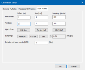
The Scan Frame parameters are not very important for the CBED calculation. However, you can set the incident probe position numerically by the scan frame offset. The position (0, 0) as set in the screenshot corresponds to the lower left corner of the structure projection and to the position of an iron column.
At this point you have setup all the parameters required for the CBED simulation. Exit the Calculation Setup dialog by clicking the [OK] button.
Running the simulations
Select Probe propagation & CBED as calculation type and start the CBED calculation by clicking on the big [Start Calculation …] button. Two additinal dialogs will appear. One dialog informs you about the calculation progress including an estimate of the remaining calculation time. The other dialog gives a preview on the calculation result, where the average electron probe intensity distribution builds up with more runs of the multislice algorithm. The progress dialog is closed automatically when the calculation is finished.
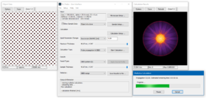
Dr. Probe GUI running CBED calculation of Fe [001] with the STEM probe located over an atomic column.
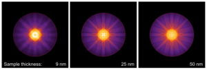
CBED patterns of bcc Fe [001] simulated with 25 mrad probe convergence for different sample thicknesses. The red circle marks 100 mrad diffraction angles.
Results
Use the controls of the Results section to navigate through the calculated images. Select [CBED pattern (k)] from the list of result types to show the CBED pattern. Use the Sample Thickness slider to browse through the thickness series.
You may also change some parameters like Sample mistilt and Illumination aperture using the quick parameter controls in the calculation section and repeat the calculations. This leads to quite strong changes of the CBED pattern as shown on the right.
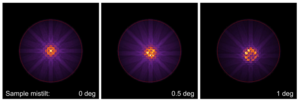
CBED patterns of bcc Fe [001] simulated with 5 mrad probe convergence for 25 nm sample thicknesses with different amounts of sample mistilt. The red circle marks 100 mrad diffraction angles.
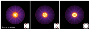
CBED patterns of bcc Fe [001] simulated with 25 mrad probe convergence for 14 nm sample thicknesses for different incident probe positions on the projected Fe [001] structure. The probe positions were as indicated by the small insets in the lower right corners of the images and are marked by the white cross. The red disks indicate the positions of Fe atomic columns.
The CBED pattern also depends on the position of the incident probe, as shown by the image on the left. You can either set the incident probe position by clicking with the mouse pointer in the object display window, or by changing the Offset position of the scan frame in the Calculation Setup.
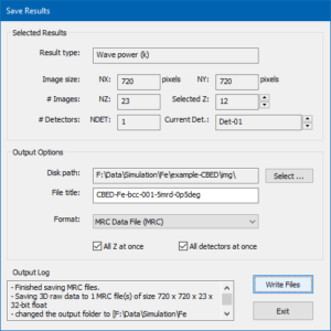
Dialog for saving multiple simulation results to files and images in various formats.
Saving simulation results
There are different ways for saving the current simulation results to files. The most convenient way is given by an additional dialog, which opens up when you press the [Save Results to File …] button. The other way is using the [Save] button in the calculation results display window.
The dialog for controlling the saving of results to files is shown in the image above and denotes information regarding the currently selected result in the upper part and lets you setup file saving options in the lower part.
For the current example, choose an appropriate destination folder (disk path) on your hard drive and enter a file name prefix (file title). Choose the MRC data file format and mark the two check boxes for saving all images of the thickness series at once. Press the [Write Files] button to initiate the saving procedure. An MRC file should now be saved to the specified disk path with the specified file title. The MRC file can be loaded in Gatan Digital Micrograph (GMS2+) by dropping the file into the application window.