In this classic example we will simulate bright-field and HAADF STEM images of cubic perovskite SrTiO3 in [001] orientation using the Dr. Probe GUI version 1.9.
For the simulation we consider a spherical-aberration corrected 300 kV scanning transmission electron microscope with 0.8 Å resolution. Let us simulate images of three detectors: a bright-field detector (BF), an annular bright-field detector (ABF), and a high-angle annular dark-field detector (HAADF). For each detector we will calculate a thickness series. This means a set of images for increasing sample thickness but otherwise constant simulation parameters. The images will be saved to files on the hard disk using the the MRC file format and in the standard image format PNG.
Quick guide to STEM image simulations
1. choose the GPU and the number of CPUs to be used (program preferences)
2. set the relevant microscope parameters
2a) accelerating voltage
2b) illumination aperture radius
2c) effective source profile and width
2d) probe aberrations
2e) detectors
3. prepare object transmission functions (setup sample)
3a) load the structure model
3b) modify the model, reorient & increase size if necessary, shift atoms to center of slices
3c) choose number of samples for the simulation grid sufficient to include largest detection angles
3d) choose number of slices matching number of atomic planes
3e) check frozen-lattice generation and set number of variants
4. stack slices periodically to maximum sample thickness
5. prepare the scanning calculation
5a) set sample tilt, thickness step size for readout, and number of repeats per scan position
5b) setup the scan frame
6. choose scan image as calculation type
7. check that the maximum thickness slider is set to the right value
8. run the multislice calculations
9. apply the source profile
10. save the results
Program preferences
Start the Dr. Probe GUI app and open the program preferences from the Setup menu. Choose a GPU if available and set the maximum number of CPU threads. It is recommended to leave 1 or 2 of the available CPUs for other system operations, e.g. the user interface.
Setup the microscope parameters
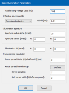
Open the Microscope Setup and proceed to the Basic Illumination Setup. Set the accelerating voltage to 300 kV, chose a Gaussian source profile of 0.04 nm HWHM, and set the illumination aperture 25 mrad (see image below). This corresponds to probe of less than 1 Å diameter without aberrations. Close the Basic Illumination Setup with the [OK} button.
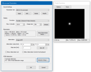
In the Microscope Parameters dialog, use the [Zero All] button to set all optical probe aberrations to zero. This corresponds to an aberration-corrected microscope, where residual aberrations play no role within the limit given by the illumination aperture.
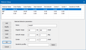
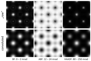
Open the Detector Setup and create a list of STEM detectors, e.g. as shown in the image below. In order to achieve similar numbers as this example, keep the maximum outer detection radius at 250 mrad. In the example below, we see a HAADF detector (80 – 250 mrad), an ABF detector (12 – 24 mrad), and a BF detector (0 – 2 mrad).
If you have problems setting up the detectors, please, download the detector setup, store it on your hard disk, and load the parameter file by clicking the [Load] button in the Detector Setup dialog.
Leave the detector setup by clicking the [OK] button. You may add the current microscope parameter setting to the list of pre-saved settings by clicking the [Add] button in the upper dialog section.
The microscope parameter setup is finished and the dialog should now look like in the image above. Acknowledge the settings with the [OK] button.
Prepare object transmission functions
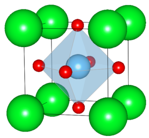
Download the initial structure model. The ZIP contains the file SrTiO3-input.cif, which describes a unit cell of SrTiO3 (STO) as published by Abramov et al. [1]. It is a cubic cell with a = 3.901 Å side length, Sr in the corners, Ti in the centre, and three oxygen atoms at the face centres according to space group symmetry P m -3 m (221), see image below.
Open the Sample Setup dialog and show the first page using Slice Creation tab. Open the Structure model by pressing the [Select File] button. A file explorer window will open and allow you to browse through your hard disk. Choose CIF file format, then select and Openthe file SrTiO3-input.cif.
The info box below the file name should now indicate that a structure has been loaded and report the dimension of the current super-cell and the number of atoms contained in this cell, as in the image on the right.
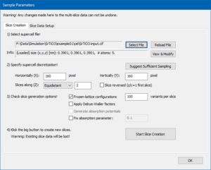
In principle a unit cell is sufficient for a simulation of a sample with periodic crystal structure. However, when considering thermal diffuse scattering in a frozen-lattice approach, we need to allow neighboring atoms to move independently. For this purpose we will now increase the structure model to 4 x 4 unit cells in the x–y plane.
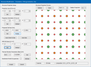
Open the Structure Modification dialog by pressing the [View & Modify] button. The dialog should display a large projection image of the STO unit cell along the [001] zone axis with a Ti-O column in the center.
We will keep this orientation but increase the size of the super-cell by a factor of 4 along x and y. Do to so, click on the [Multiply] button and enter the multiplication factors for x = 4, y = 4, and z = 1 in the small setup dialog. Acknowledge the setting by pressing the [OK]. As a result, the structure projection should now show 16 projected unit cells of STO [001] in a super-cell of 1.5604 nm × 1.5604 nm × 0.3901 nm size as shown by the screenshot on the right.
By selecting the other two projection options for the structure display (x-z and y-z) in the top-right corner of the dialog you will notice, that the structure consists of two atomic planes along the projection direction (z). We always want to represent the individual atomic planes by the slicing of the structure in the following step, where the super-cell is divided into equidistant slices along z. By making one slice for each atomic plane, the diffraction calculations will reproduce higher-order Laue zone interferences correctly. In the present example we therefore create 2 slices.
It is advantageous for numerical reasons to place the atomic planes in the centre of the future slices (avoids round-off errors). In the present example this requires a shift of 0.25 of the cell size along z: Click the [Set] button in the section Shift All Atoms [u’v’w’] and enter x = 0, y = 0, z = 0.25 as shift vector in the small dialog.
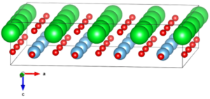
(Optional) You may save the modified structure model to disk in form of a CIF or CEL file. For your convenience a backup of the modified structure is available by download. A display of the extended structure model generated by the program VESTA is shown in the image on the right.
Press the [Accept] button and return to the Slice Creation.
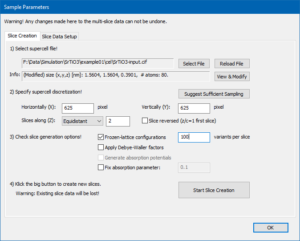
Now, the Slice Creation page displays the modified cell size and number of atoms in the info box. This is the super-cell we’re going to use in the multislice simulation.
First choose the Equidistant slicing scheme, then set the numerical sampling of projected potentials and the number of slices by clicking on the [Suggest Sufficient Sampling] button. The number of pixels in the projection plane is set to 625 × 625 and the number of slices is 2, corresponding to the 2 atomic planes along z of our structure model. This grid size is sufficient for calculating the high angle scattering up to more than 250 mrad, comprising the complete angular range of the previously defined detector setup.
Check to use Frozen-lattice configurations and set the number of variants per slice to 100. The Slice Creation page should now look like in the image below.
Start the slice creation by clicking the big button in the lower right area of the dialog and wait until the calculation has finished. The calculation uses as many CPU threads as set in the program preferences earlier and should be finished in less than a minute on modern desktop PCs.
Stack slices to maximum sample thickness
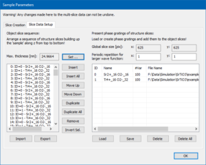
Switch to the [Slice Data Setup] tab, which lists now two slices in each of the two list boxes. The left list box shows the object slice sequence consisting currently of a Sr-O slice and a Ti-O2 slice, while the right list shows the available phase grating data.
If you want to save the phase gratings to your hard disk, click the [Save] button below the right list. Another dialog will open, asking for an existing directory and a file name for storing the data. Change the names as appropriate for you and click the [OK] button to start the file saving.
(Optional) In case of problems with one of the previous steps, you may download the slice phase gratings, save them to your hard drive and load them in Dr. Probe using the [Load] button below the list on the right side.
Our sample still has a maximum thickness of one SrTiO3 unit cell. Change this by clicking the [Set] button and entering 25 nm.
The left list is now filled with a periodic sequence (0, 1, 0, 1, …) of the phase gratings contained in the right list. The stack contains a total number 128 slices corresponding to 24.9664 nm sample thickness.
(Optional) In case of problems with the setup of the object slice sequence, you may download the object slice sequence setup from this website, save it to your hard disk, and load it in Dr. Probe by clicking the [Import] button below the list on the left side.
With this step, the sample setup is finished. Click [OK] in the lower right.
Returning to the main dialog, you will find a short report of the sample setup Status Information, i.e. the grid size, sample thickness and number of slices. The latter is also reflected by the slider for Maximum Thickness in the Calculation section.
You can inspect the current sample setup, the slices, and phase gratings by checking Show Sample Data in the Input section. This will open the Object Data display window. The Maximum Thickness slide can be used for browsing through slice specific data. Take care to move it back to the rightmost position when you are finished.
Prepare the scanning calculation
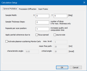
Open the ‘Calculation Setup‘ in order to set a few final parameters for the STEM image simulation.
In the General Multislice section we set the sample mistilt to 0° for both directions. Feel free to play with this parameter later. Let’s set the sample thickness step to 2 slices. With this setting, Dr. Probe will evaluate the detectors after every 2 slices, periodically up to the maximum sample thickness of 25 nm. The step of 2 slices corresponds to 0.3901 nm thickness. We will receive 65 images per detector, including an image from the entrance plane of the crystal.
Set the Repeats per scan position to 1. With this setting, we calculate only one multislice per scan pixel. For very accurate simulations about 10 repeats per pixel are recommended. You will see strong intensity variations between neighboring scan positions, which will be reduced later by the convolution with the source distribution function.
For simplicity of example, we leave all the check boxes for partial coherence and plasmon scattering unchecked.
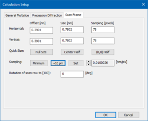
In the Scan Frame section, we use the shortcut button [Center Half] to define the scan frame of half the size of the phase gratings (2 × 2 unit cells), centered in the simulation box. Keep the scan frame rotation at 0°.
Press the button [∼10 pm] to set the number of scan positions to 78 × 78, realizing an approximate step size of 10 pm.
Acknowledge the calculation setup by clicking the [OK] button and return to the main dialog of the Dr. Probe user interface.
(Optional) You may download the user interface setup, store it on your hard drive, and load it via the File / Load Parameters … menu. This will set all parameters of the UI (except phase gratings) similar to those used in this example.
Run the simulation
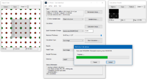
Before starting the actual simulation, check the current setup by taking a look at the present sample data: The object data display shows the scan frame by its fast (x, solid) and slow (y, dashed) scan axes. Scan positions are marked by dots. The maximum thickness slider should be in rightmost position (slice #127).
Select the calculation type Scan image and start the calculation by clicking on [Start Calculation …]. Two additional dialogs will appear. One dialog informs you about the progress of the image calculations. The other dialog gives a preview of the results for the first detector at maximum thickness. The calculations will use the GPU and number of CPU threads in parallel, according to the program preferences. This will take a few minutes on commercial desktop PCs.
The progress window is closed automatically when the calculations are finished. Use the controls of the Results section to navigate through the calculated images. Browse through the images extracted at different sample thickness with the slider. Look at images of different detectors by choosing from the Detectors list.
The “raw” STEM images show very sharp intensity peaks at the atomic columns with high contrast. This is because the resolution limiting effect of the partial spatial coherence has been omitted so far. By clicking on the [Apply Source Profile] button all images are convoluted by the effective source profile. The resulting images appear with a significantly smoothed and lower contrast as shown in the figure below.
Save simulation results
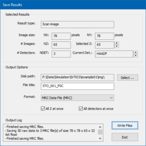
Press the [Save Results to File …] button to open a special dialog for saving the data.
Here you find information concerning the currently selected results options for saving the images to files in different formats.
For the current example, choose an appropriate destination folder (disk path) on your hard drive and enter a file title. Choose the MRC data file format and mark the two check boxes for saving all images of the thickness series and images for all detectors at once, respectively. Press the [Write Files] button.
Three MRC files are saved, each containing the thickness series simulated for one STEM detector. You may use Gatan Digital MicrographTM for visualizing and inspecting the results of the STEM image simulation. The software supports drag & drop for MRC files.
Repeat the saving of results using the image format PNG. Now 65 PNG files will be saved to the selected disk path for each detector. An index suffix is added to the file title distinguishing the images of the thickness series, where “001” is the image at zero thickness and “065” is the image at 25 nm thickness. The contrast and color settings of the results display window are used for the image creation.
Download the results of this simulation example for comparison with your own calculation results.
References
1. Yu.A. Abramov, V.G. Tsirel’son, V.E. Zavodnik, S.A. Ivanov, and I.D. Brown, Acta Cryst. B 51 (1995) p. 942. doi: 10.1107/S0108768195003752


