FEI Helios NanoLab 460F1 FIB-SEM
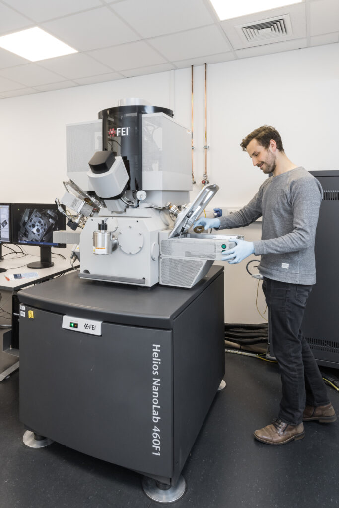
The FEI Helios NanoLab 460F1 is a highly advanced dual beam FIB-SEM platform for imaging and analytical measurements, transmission electron microscopy (TEM) sample and atom probe (AP) needle preparation, process development and process control. For these purposes, the FEI Helios NanoLab 460F1 combines an ElstarTM UC technology electron column for high-resolution and high material contrast imaging with the high-performance TomahawkTM ion column for fast and precise sample preparation. The FEI Helios NanoLab 460F1 is additionally equipped with the MultiChemTM gas delivery system, an EasyLiftTM nanomanipulator, a cooling trap, an inert gas transfer (IGT) holder loadlock, a quick loader, a FlipStage 3TM, an EDX-System and an STEM III detector. This instrument is one of the few dual beam systems which combine an IGT holder loadlock with a FlipStage 3+TM EasyLiftTM nanomanipulator. Typical examples of use and technical specifications for the instrument are given below.
The FEI Helios NanoLab 460F1 was funded by the German Federal Ministry of Education and Research (BMBF) via the project SABLE (SABLE-Skalenübergreifende, multi-modale 3D-Bildgebung Elektrochemischer Hochleistungskomponenten) under support code 03EK3543.
Typical Applications and Limitations of Use
The configuration of the FEI Helios NanoLab 460F1 allows a variety of advanced imaging and preparation techniques to be applied to wide bunch of solid state materials. These techniques include TEM sample preparation (normal- and backside milling) without breaking the vacuum (with Flipstage 3), STEM imaging on thin TEM samples (with STEM 3 detector), slice and view operation (automatic), needle preparation for tomography, atom probe sample preparation, plan-view preparation and the preparation of lamellas on heating chips for TEM annealing experiments. Making use of the IGT-loadlock, even samples who are not allowed to be supposed to air can be prepared on any of the previously described ways except needle and atom probe preparation.
The FEI Helios NanoLab 460F1 is not intended for the investigation of aqueous, ferromagnetic or organic samples without further discussions with both of the instruments officers and the ER-C general management.
Sample Environment
The vacuum is about 10-7 mbar under normal operating conditions.
Technical Specifications
| Electron landing voltage | 20 V … 30 kV |
| Ion landing voltage | 500 V … 30 kV |
| Electron beam current | ≤ 0.1 µA |
| Ion beam current | ≤ 65 nA |
| Electron source | Schottky thermal field emitter |
| Resolution optimal WD(SEM) @ 2 … 15 kV | < 0.6 nm |
| Resolution optimal WD(SEM) @ 1 kV | < 0.7 nm |
| Resolution optimal WD (SEM) @ 200 V with beam deceleration | < 1.5 nm |
| Resolution (STEM) | < 0.6 nm |
| Ion source | Gallium liquid metal |
| Resolution (FIB) @ 30 kV | < 4 nm |
| Resolution (EDX) | < 30 nm |
Specimen Stages
| Flipstage 3 with in situ STEM 3 detector |
| 5 axis all piezo motorised |
| 100 mm XY motion |
| IGT-Loadlock |
| Quick Loader |
EDX System
| TEAM software for measurement and analyses |
| “Octane Super” Detector |
| Active Area: 60mm² |
MultiChem Gas Delivery System
| Pt, C, W for deposition |
| TEOS for insulator deposition |
| H2O etching gas |